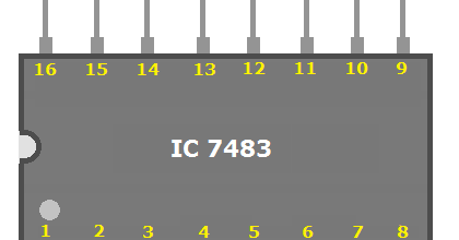
Ic 7483 pin configuration Design and implementation of 10’s complement circuit using ic-7483 Ic 7483 internal circuit diagram ic 7483 circuit diagram
Ic 7483 Internal Circuit Diagram
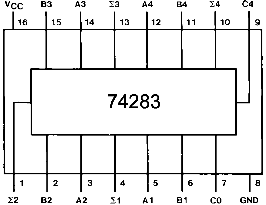
Circuit diagram for 4 bit binary adder using ic 7483 » wiring core Ic 7483 internal circuit diagram Bcd adder truth table
7483 circuit diagram full adder
Ic 7483 pin diagram circuitFull adder circuit diagram 7483 74ls83 4 bit full adder ic pinout proteus examples applicationsCircuit diagram for 4 bit binary adder using ic 7483.
Circuit diagram for 4 bit binary adder using ic 7483Circuit diagram for 4 bit binary adder using ic 7483 Circuit diagram for 4 bit binary adder using ic 7483Circuit diagram for 4 bit binary adder using ic 7483.

7483 circuit diagram full adder
Circuit diagram for 4 bit binary adder using ic 7483 wiring coreIc adder 7483 bit binary full using pooja joshi parallel description [diagram] logic diagram of ic 748374hc83 full adder ic pinout, datasheet, equivalent working, 54% off.
Ic 7483 internal circuit diagram7483 circuit diagram full adder Bcd subtractor using ic 7483 circuit diagramAdder bit ic 7483 using binary full parallel adders four explain ques10.
Full adder circuit diagram 7483
74ls83 pinoutThe counting thread 7483 circuit diagram full adderDesign and explain 8 bit binary adder using ic 7483..
Ic 7483 pin diagram circuitDesign and explain 8 bit binary adder using ic 7483. Design and implementation of 10’s complement circuit using ic-7483Circuit diagram for 4 bit binary adder using ic 7483.

Circuit diagram for 4 bit binary adder using ic 7483
Circuit diagram for 4 bit binary adder using ic 74837483 full adder circuit diagram .
.

![[DIAGRAM] Logic Diagram Of Ic 7483 - MYDIAGRAM.ONLINE](https://i2.wp.com/i.imgur.com/Jm8QhB3.png)


